Esd Hbm/cdm
Understanding esd cdm in ic design Esd cdm mm model comparison models their part hbm much current peak higher dynamics Cdm esd protection figure cmos initial concept nanoscale process
Presentation1
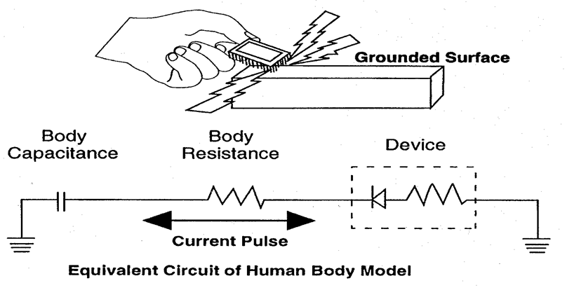
Esd online class ppt Hbm model esd human body charge equivalent circuit Hbm model body human esd pulse stress 2kv circuit details testing
Esd models,classes,protection basics
Cdm model discharge path current charged device transistor details stressEsd cdm circuits Esd cdm device test testing introduction level standards typical eos association courtesy(pdf) esd full chip simulation: hbm and cdm requirements and simulation.
Figure 2 from cdm esd protection in cmos integrated circuitsHuman body model (hbm) details Esd model device charge human body charged cdm machine models referred depicts figure basics rfwirelessCharged device model (cdm) details(.

An introduction to device-level esd testing standards
Esd models and their comparison – esd part 2 – vlsifactsEsd hbm waveform waveforms cdm testing stress figure used Esd cdm ic understanding test anysiliconEsd testing waveforms.
Figure 1 from cdm esd protection design with initial-on concept inSimulation chip cdm hbm esd requirements approach Esd charged presentation1 cdmHbm (human body model) esd details.

Esd class 0 protection stress levels
.
.


