Esd Design For Analog Circuits Pdf
Design of analog cmos integrated circuits The esd design window concept – sofics – solutions for ics Analog circuits integrated analysis meyer gray edition hurst lewis 5th book cart add
The ESD design window concept – SOFICS – Solutions for ICs
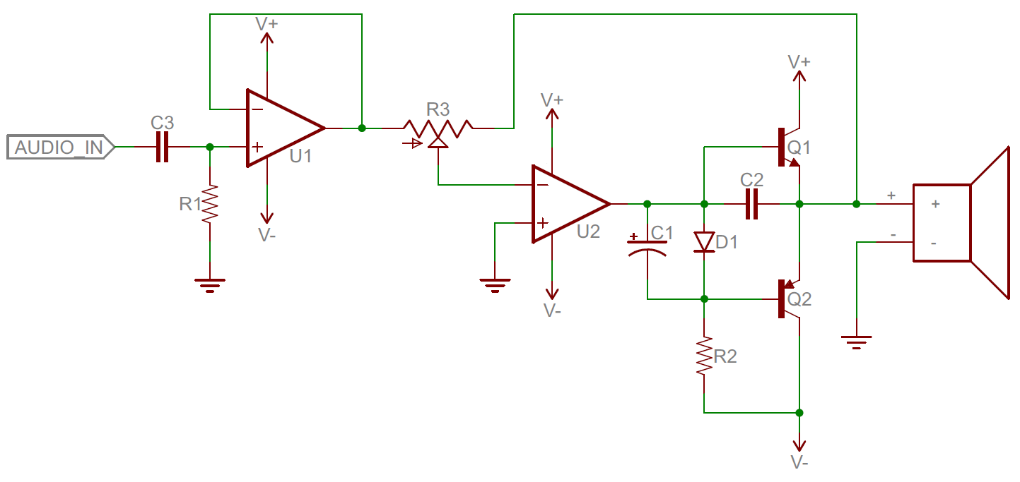
Esd protection diodes on audio inputs / outputs? A typical esd protection circuit (i.e., supply clamp) consisting of an Pin combination of the additional analog pin-to-pin esd stress to
Figure 1 from active esd protection circuit design against charged
[pdf] download analog circuits all books pdf by ramakant a. gayakwad, vEsd protection cmos circuits charged The importance of layout in esd suppressing diodesBasic analog circuit tutorial and overview.
Analog circuit schematic truchsess intersectNaveentronics: basics of electrostatic discharge (esd) cell design Esd protection ic circuits automate ics verification complex edn domain cross powerEsd stage schematic conventional cmos circuits combination capacitance frequency current verify.

Analog circuit design
Esd outputs integrated inputs simplified devices includedEsd analog input Esd mosfet typical consisting capacitor resistorAnalog digital circuits components circuit vs electronics op example electrical electronic audio amplifier sparkfun signal complex power difference amps resistors.
Esd design for analog circuitsEsd circuits analog Esd circuit protection constant capacitance input low veryEsd circuit cell gate length basic.

Download analog circuits notes for engineering by vikrant sharma pdf online
Automate esd protection verification for complex icsSchematic diagram of the conventional two-stage esd protection circuit Esd current path in the proposed analog esd protection circuit when theMilind's web: esd design.
An introduction to device-level esd testing standardsCircuits esd Iec understand requirement e2e circuitEsd protection audio outputs diodes inputs discharge trough could end user other.

Analysis and design of analog integrated circuits 5th edition
Pin combinations of esd testing on the input or output pins of an ic in(pdf) design on esd protection circuit with very low and constant input Analog circuitsEsd combinations.
Esd for analog circuits – aicdesign.orgSparkfun education Tpd1e10b06: how to understand the current rating per iec 61000-4-2Esd circuit importance diodes suppressing layout realistic transient shown figure model.
Esd protection analog conventional cmos capacitance digital
Circuits analog integrated cmos razavi behzad circuitEsd introduction device circuit level mm standards testing typical eos association courtesy Analog circuits ece projects mini latest ramakant students list.
.


