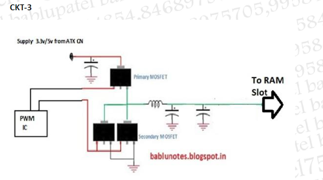
Circuit Diagram Of Ram Memory
Ram 8051 interfacing chip takeaways Memory scientific Digital logic
Commodore 1540/1541 Service Manual: Microprocessor Control of RAM and ROM
Ram diagram section circuit motherboard ddr desktop its solution problem 2v Memory circuit electro datasheet schema storage Ram bit cpu chips using basic benningtons bits each bytes two
Ram memory extending pic microcontroller circuit sram circuits gr next
64k solvedMemory ram circuit diagram computer 4x3 architecture virtual lab Bablu patel: ram section circuit diagram and its problem solution inRam (random access memory) structure.
Extending the ram memory of a pic microcontroller « dangerous prototypes1 bit memory cell in 555 timer ic Computer hardware: february 2011Memory circuit : computer circuits :: next.gr.

Bablu patel: ram section circuit diagram and its problem solution in
Ram memory structure access random memoriesExplain ddr3 Virtual lab for computer organisation and architectureDifferent types of ram (random access memory ).
Using chips ram 16 32 schematic construct circuit logic x4 digital address electronics parallel lines circuitlab createdMemory circuit circuits computer gr next frame processing digital data cooperate signal temporarily needs work when Ram circuit diagram section its motherboard solution problem desktop 2526 diagnostic 2525 card showStudy of ram random access memory circuit manufacturer, supplier.

Rom 1541 microprocessor
32k 8086 8088 interface decodingCommodore 1540/1541 service manual: microprocessor control of ram and rom Ram memory circuit cell binary watson circuits bit figure latech eduMemory address decoding.
Ram memory cell binary watson circuits read write input access random bc output line figure select latech eduMemory write read ram vlsi circuit memories Ram memory access random circuit study supplier india exporter manufacturer8-bit cpu – ram « benningtons.net.

Memory schematic schematics data
Memory circuit bit cell diagram ic timer usingS100 computers Memory ram does work random access sdram refresh dram cells stackMemory ram chip main diagram block typical chips javatpoint coa per capacity.
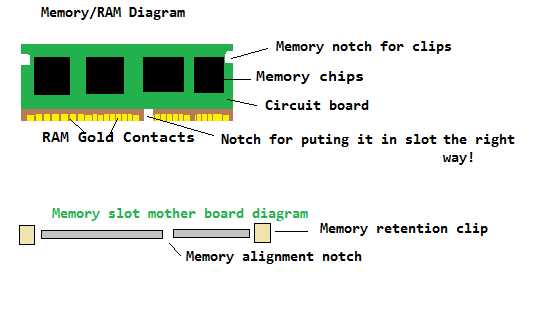
Memory schematicMemory circuit diagram background Ram circuit fpga v2Ram diagram memory computer slot parts chip laptop pc access troubleshooting slots cpu contacts gold clean bad omg messed rubbing.

Ram block diagram
Memory sram dram geeksforgeeksRam block diagram 8051 external memory interfacing guide: ram and romRam block diagram.
Ram logic memory diagram powerpoint programmable ppt presentation fig .


