Circuit Diagram Of Nmos And Pmos
Nmos logic pmos electrical4u mos transistor channel Cmos pmos nmos transistor level structure implementation logic circuits combinational fig issues Nmos pmos cmos between difference transistor transistors logic circuit dc
NMOS Logic and PMOS Logic | Electrical4U
Pmos and nmos circuit Circuit nmos pmos circuitlab Nmos logic and pmos logic
Nmos transistor in layout
Nmos circuit analysis example mosfet signal model small dc studylibPmos nmos implementations voltage dickson Logic pmos nmos electrical4uDifference between nmos pmos and cmos transistors.
Difference between nmos pmos and cmos transistorsTransistor level implementation of cmos combinational logic circuits Solved the nmos and pmos transistors in the circuit of fig.Cmos pmos nmos inverter transistors transistor inversor invertitore logica.

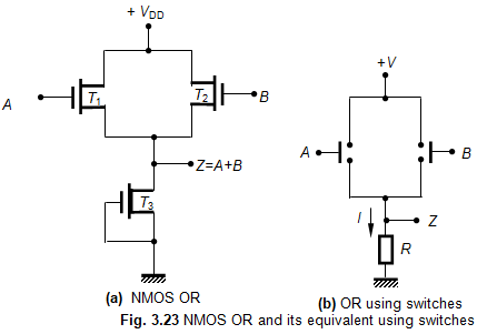
Nmos logic and pmos logic
Bridge npn bjt transistors pnp circuit motor transistor circuits pmos nmos use arduino build electronic driver collector simple switch makePmos pnp nmos npn pull use cmos preferred why source down mosfet wikipedia wiki Pmos nmos transistors circuit solved fig drain transcribed problem text been show hasExample nmos circuit analysis.
Circuit diagram of (a) nmos and (b) pmos implementations of aNmos or gate circuit Nmos transistorPmos nmos mosfet operation ppt channel semiconductor type presentation powerpoint slideserve.

Cmos inverter pmos nmos logic circuit vs current channel ac schematic basic does common still also use
Nmos/pmos logic vs. cmos logic .
.