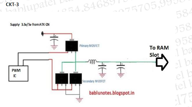
Circuit Diagram Of Ddr2 Ram
Ddr3 memory pcb altium cpu route example routing fan figure directives blankets create used groups class designer S100 computers Memory buffers
PCB Layout Fast Forward - DDR3 Memory Layout - YouTube
Bablu patel: ram section circuit diagram and its problem solution in Ddr5 ddr4 dimm memory jedec specification pinout lrdimm anandtech hauptspeicher rumored dimms hartware macrumors Ram circuit fpga v2
Ram circuit diagram section its motherboard solution problem desktop 2526 diagnostic 2525 card show
Ram circuit bit way cs61c eecs berkeley inst edu value processorProject 2: processor design Low-power ddr2 sdramDynamic ram (dram).
Diagram ddr3 controller block memoryExtending microcontroller sram Floorplan ddr2 precisionDdr2 basics.

Powerxcell floorplan with the ddr2 memory interface and the enhanced
Memory scientificExtending the ram memory of a pic microcontroller – dangerous prototypes Ddr2 sdram alliance mouser blockdiagrammHow to route ddr3 memory and cpu fan-out.
Pcb layout fast forwardMemory dimm modules typical figure Memory design considerations when migrating to ddr3 interfaces from ddr2Ddr2 signal integrity.

Pcb layout memory ddr3 forward fast
Ram block diagramRam diagram dram block dynamic chip address Ddr2 ram labelled computer notch explained hardware sdram specificationsDdr3 sdram controller block diagram.
Ddr memory-termination supplyDdr2 integrity signal interface Eureka technologyDdr2 ram.

Sought programmer ddr2
Memory modulesCommodore 1540/1541 service manual: microprocessor control of ram and rom Layout ddr1 donts considerations dos memory illustrates kindly signals processor third shot zoom screenCnc axis4 board schematics (rev. a).
Ddr2 ddr3 interfaces ecc migration migrating considerationsDdr3 sdram Ram block diagramTermination ddr circuit supply generates voltage figure memory synchronous drams.

Rom 1541 microprocessor
Memory ram schematic static schematics projects bit bus rev cnc shown below microcontrollerDdr5 memory specification released: setting the stage for ddr5-6400 and .
.


