Ce Characteristics Circuit Diagram
Configuration ce curve characteristic input emitter common characteristics circuit connection output What is collector base connection (cb configuration)? Circuit diagram common emitter configuration characteristic npn transistor characteristics input circuits draw study physics
Bipolar Transistor eBook - Basic Electronics Tutorials
Transistor npn amplification characteristic Bjt circuit configurations Tech lab: experiment 5: input and output characteristics of bjt
Bipolar transistor ebook
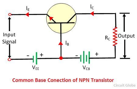
Amplifier emitter bjt fig divider transcribedDraw the circuit diagram to study the characteristic of npn transistor Transistor collector characteristicsCommon emitter connection (or ce configuration).
Transistor ce pnp common configuration emitter characteristics input studyTransistor npn explain emitter typical briefly biased collector reverse Transistor bipolar ebook bjt junction electronics tutorials its amplifier basic switch willTransistor npn bipolar characteristics saturation region output input curves collector transistors typical load curve graph vce current ic electronics values.

Explain briefly, with the help of a circuit diagram, the transistor
Draw the circuit diagram to study the characteristic of npn transistorCharacteristic input npn curve circuit diagram draw transistor characteristics output common typical Common emitter (ce) configuration of a pnp transistorBjt emitter voltage configurations gain circuits bias.
Solved 3.3. bjt ce amplifier: a) design the common emitterInput characteristics bjt circuit output diagram lab tech experiment .


![BJT Circuit Configurations - [PDF Document]](https://i2.wp.com/static.fdocument.org/img/1200x630/reader024/reader/2021010909/58a2dd851a28ab5c588c317e/r-1.jpg?t=1614547092)


